Intel SoMs & FPGAs
Performance and Efficiency for Cost-Sensitive Applications
Agilex™ 5 FPGA and SoC FPGA E-SeriesManufactured using Intel 7 technology and delivers better performance-per-watt, low power, and smaller form factors for midrange FPGA applications. |
||
|
Up to 1.6X better performance-per-watt vs. 16 nm node competitors. |
Optimized for Power and SizeUp to 50% lower total power consumption vs. Cyclone® V FPGAs. |
Up to 2.5X fabric performance compared to Cyclone® V FPGAs. |
 |
||
Power-Efficient PerformanceBuilt on Intel 7 technology, E-Series FPGAs deliver superior power-efficient performance at 1.6x better performance-per-watt1 compared to the competing 16 nm FPGAs and have the first asymmetric Arm application processor cluster to deliver better HPS energy efficiency. |
Unmatched ReliabilityImplement reliable and secure systems with functional safety (FuSa) and an integrated security device manager offering advanced security features and leveraging Intel advanced manufacturing capabilities for supply resiliency and best-in-class lead times with predictable and reliable delivery. |
Innovative, Scalable, and AdaptableMeet your diverse application needs with a broad set of IP and connectivity options with a wide density range (50KLE-656KLE) to scale device size and support the variety of I/O standards in edge and embedded sensors configurable in a single FPGA device. |
Key Features |
||
Second Generation Intel® Hyperflex™ FPGA ArchitectureAdvantages include higher throughput, improved power efficiency, greater design functionality, and increased designer productivity. |
Enhanced DSP with AI Tensor BlockOffers up to 56 peak INT8 TOPS with FPGA AI Suite support to enable push-button flow from industry standard frameworks to FPGA bitstream. |
Advanced SecurityBuilt with robust security features, the Secure Device Manager (SDM) and firmware ensure the confidentiality and integrity of the device. |
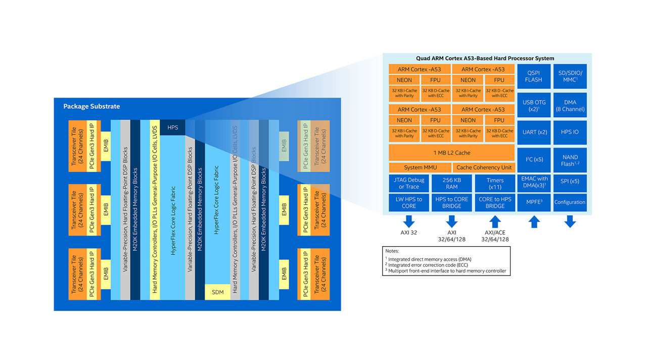
Intel® Stratix® 10 SX SoC FPGAIntel® Stratix® 10 SoC FPGA combines a quad-core ARM Cortex–A53 MPCore hard processor system with the revolutionary Intel® Hyperflex™ FPGA Architecture to deliver the embedded performance, power efficiency, density, and system integration necessary for embedded applications. |
||
 |
||
Enabling Designers to Do More with HPS While Balancing Power EfficiencyWith an embedded hard processor system (HPS) based on a quad-core 64-bit Arm Cortex -A53, the Intel® Stratix® 10 SoC devices deliver power-efficient, application-class processing and allow designers to extend hardware virtualization into the FPGA fabric. |
Achieve High Levels of System IntegrationIntel® Stratix® 10 SoC FPGA empowers the USR in the ARM ecosystem. ARM's next-generation 64-bit architecture (ARMv8) enables hardware virtualization, system management and monitoring capabilities, and acceleration pre-processing. The ARM Cortex-A53 processor supports 32-bit execution mode and board support packages for popular operating systems, including Linux, Wind River’s VxWorks, Micrium’s uC/OS-II and uC/OS-III, and more. |
Achieve High Designer Productivity with Optimized FPGA and SoC FPGA SoftwareOptimized for multi-million logic elements (LE), the Virtual Platform streamlines design iterations, fostering early software development. C-based design with Intel® FPGA SDK for OpenCL™ offers an easy-to-implement environment on SoC FPGA. The Intel® SoC FPGA Embedded Development Suite (EDS) enables debugging, profiling, and whole-chip visualization with the ARM* Development Studio 5 (DS-5) FPGA Edition Toolkit. |
Applications |
||

Data Center AccelerationThe Intel® Stratix® 10 SX SoC FPGA accelerates data centers by integrating FPGA fabric with ARM processors. This allows for versatile applications, including real-time processing, protocol handling, AI (Artificial Intelligence) inference, security, and customized I/O interfaces. It combines FPGA's parallel processing with embedded processors for tasks like edge analytics, networking, and optimized data management, making it a key component for diverse workloads in data centers. |

Industrial AutomationThe Intel® Stratix® 10 SX SoC FPGA enhances industrial automation with real-time control, protocol handling, signal processing, motor control, safety features, vision processing, high-speed I/O, protocol conversion, cybersecurity, and fault detection, enabling intelligent, responsive systems while ensuring compatibility and efficient data processing. |

Image and Video ProcessingThe FPGA fabric can support tasks like image enhancement, compression, decompression, and object recognition in applications like medical imaging, video processing, and computer vision. At the same time, the ARM cores handle higher-level processing. |
Key Features |
||
Hard Processor System (HPS)At the heart of the HPS is a highly efficient quad-core ARM Cortex-A53 processor cluster, and this processor is optimized for ultra-high performance per watt, which reduces power consumption. The HPS includes a System Memory Management Unit, Cache Coherency Unit, a hard memory controller, and a rich feature set of embedded peripherals. |
Digital Signal Processing (DSP)With Intel® Stratix® 10 devices, DSP designs can achieve up to 8.6 Tera floating point operations per second (TFLOPS) of IEEE 754 single-precision floating-point operations. |
Secure Device Manager (SDM)SDM controls key operations, such as configuration, device security, single event upset (SEU) responses, and power management. It creates a unified, secure management system for the entire device, including the FPGA fabric, hard processor system (HPS) in SoCs, embedded hard IP blocks, and I/O blocks. |
Cyclone® 10 GX FPGAThe Cyclone® 10 GX FPGA is built on a high-performance 20 nm process, offering a performance advantage for cost-sensitive applications. |
||
 |
||
Enhanced Core Architecture with High-Bandwidth Integrated TransceiversBuilt on 20 nm process technology and programmable with the advanced Quartus® design environment, achieve twice the performance of previous-generation Cyclone V FPGAs along with 12.5 Gbps chip-to-chip transceiver I/O and 6.6 Gbps backplane support. |
Improved Efficiency and Timing ClosureThe Adaptive Logic Module architecture – same as previous-generation FPGAs – allows the efficient implementation of logic functions, simplified conversion of intellectual property (IP) cores between the device generations, and improved timing closure in devices. |
Advanced Power SavingCyclone 10 GX FPGAs offer a comprehensive set of advanced power-saving features with power-optimized MultiTrack routing and core architecture reducing power consumption. |
Use Cases and Applications |
||

Embedded Video and Image Processing ApplicationsJPEG XS compression can be used in applications that previously transported uncompressed image and video data – enabling systems to offer higher quality resolution at faster frame rates. |

Design Flexible 4K Video FPGA Systems with DisplayPort™ 1.4 ConnectivityCreate custom video processing applications using the high-quality, plug-and-play portfolio of in-house video processing IP from Intel® FPGA VIP IP Suite. |
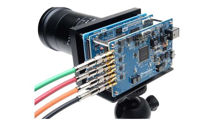
Smart and Easy Way to Develop Machine Vision Systems for High-PerformanceEasy Machine Vision Camera (EasyMVC) is designed to eliminate the hurdles of machine vision system development. |
Key Features |
||
Transceivers12.5 Gbps chip-to-chip transceiver support, 6.6 Gbps backplane support along with hard PCI Express (PCIe) IP supporting PCIe 2.0. |
External Memory InterfaceHigh-performance external memory interface with up to 1,866 Mbps DDR3. |
General Purpose I/O and DSPsEach I/O bank contains GPIOs featuring 1.434 Gbps LVDS I/Os and support a wide range of I/O interfaces.IEEE 754-compliant hard floating-point digital signal processing (DSP) blocks. |
Available Models
| Model | FPGA | RAM | SPI Flash |
Form factor |
DSPs | Ethernet | Temperature Range |
|---|---|---|---|---|---|---|---|
| TEI0001-04-DBC87A | MAX 10 | 8 MB | dual insdie | 6.15 x 2.5 cm | - | - | extended |
| TEI0001-04-FBC84A | MAX 10 | 32 MB | dual insdie | 6.15 x 2.5 cm | - | - | extended |
| TEI0003-03-QFCT4A | Cyclone 10 LP | 8 MB | 8 MB | 6.15 x 2.5 cm | 66 | - | commercial |
| TEI0006-04-ALE13A | Cyclone 10 GX | 128 MB | 256 MB | 6 x 8 cm | - | 1 Gb | extended |
| TEI0006-04-API23A | Cyclone 10 GX | 2 GB | 256 MB | 6 x 8 cm | - | 1 Gb | industrial |
| TEI0022-03 | Cyclone V | 1 GB HPS 1 GB FPGA |
32 MB HPS 32 MB FPGA |
13 x 16 cm | - | 1 Gb | commercial |
| TEI0050-01-AAH13A | Cyclone V E | 8 MB | 8 MB | 2.5 x 7.07 cm | - | - | commercial |
| TEI1000-01-A1I11-A | Stratix10 SX | 1 GB DDR4 | 64 MB | 6 x 8 cm | 648 | - | industrial |
| TEI0187-01-T4E11-A | Agilex 5E | 2 GB DDR4 | 256 MB | 5.2 x 7.6 cm | 1,692 | 1 Gb | industrial |
PRICING, AVAILABILITY AND ORDERING
Email